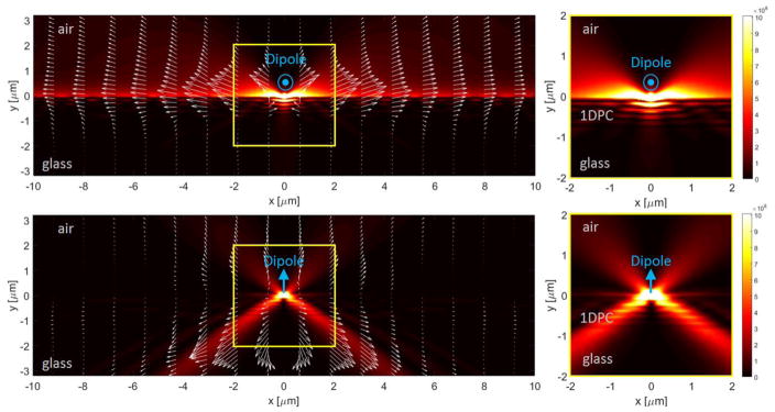
Figure 9.
Numerical FEM model of the |E|2 (false color map) and Poynting vector (arrow plot) distributions of the radiation emitted by a dipole embedded within a PVA layer, at 5 nm from the 1DPC surface. Dipole with horizontal orientation showing S-polarized emission coupled to BSW is shown in the top panel. Dipole with vertical orientation showing P-polarized emission with no coupling to BSW is shown in the bottom panel. Emission wavelength is 420 nm. Calculations are performed using Comsol Multiphysics software. Color scale for |E| 2 is linear. Arrow length is proportional to Poynting vector on a logarithmic scale.

