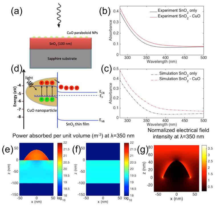
FIG. 3.
(a) Diagram of the setup for the FDTD simulations. A SnO2 film thickness of 100 nm was used for the simulations with and without CuO NPs. The CuO NP clusters were modeled as elliptic paraboloids with heights of 45 nm and diameters of 75 nm. The CuO NPs were randomly distributed on the SnO2 film with an average surface density of 65 μm−2. The size and average density values of the NPs were based on AFM measurements of the real devices. (b) Measured and (c) FDTD simulated absorption spectra of the SnO2 and SnO2-CuO films. (d) Schematic band diagram illustrating the hypothesized electron transfer process in the CuO-SnO2 nanoheterojunctions under irradiation. (e) Spatial cross-section of simulated power absorbed per unit volume at λ = 350 nm in a single CuO NP on a SnO2 film and (f) in a bare SnO2 film. (g) Spatial cross-section of simulated normalized electrical field intensity at λ = 350 nm for a single CuO NP on a SnO2 film.

