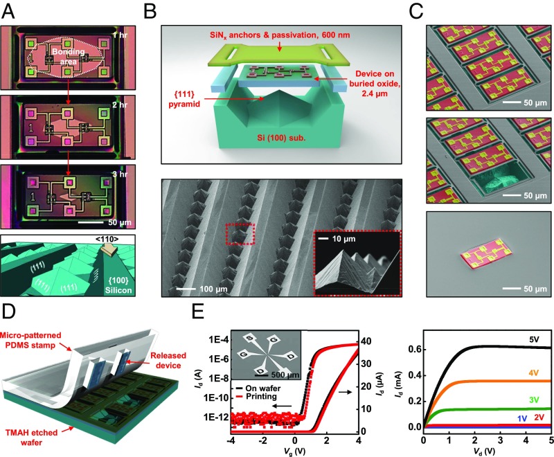
Fig. 2.
Aspects of release of thin, transient CMOS devices based on anisotropic etching of the Si (100) handle wafer. (A, Top) Optical micrographs collected at 1 h, 2 h, and 3 h after undercut etching to release a representative device (n-channel MOSFET). (A, Bottom) Schematic illustration of the anisotropic etching profile associated with the Si (100) substrate. (B, Top) Schematic exploded view illustration of the structural configuration of a unit cell in an array of devices after complete release. The etched areas are bounded by Si (111) planes, with freely suspended devices tethered by SiNx anchors across the trenches. (B, Bottom) SEM images of etched structures in the Si (100) handle wafer after removal of the released devices. (C) SEM images of an array of devices (colorized using a scheme similar to the scheme in Fig. 1 for ease of viewing), shown in sequence, after undercut etching (Top), after removal of a single device from the handle wafer (Middle), and after transfer printing of this device onto a target substrate (Bottom). (D) Schematic illustration of the process for transfer printing with a PDMS stamp. (E, Left) Linear and log-scale transfer characteristics of an n-channel MOSFET before (black) and after (red) transfer. (E, Right) Output characteristics of the same transistor. Id, drain current; Vg, gate voltage.

