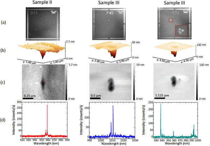
Figure 3.

Examples of different morphological features observed via atomic force microscopy, correlated to quantum dot positions and their photoluminescence spectra (a) EMCCD images of the photoluminescence from QDs and reflected light by the alignment marks (metallic crosses), acquired by illuminating three different fields of two different samples (sample II in the first column and sample III in the second and third columns) simultaneously with both the red and near-infrared LEDs, at a temperature of 4 K. The inset in the third image represents a zoom-in of the area marked by the dashed red lines in the QD photoluminescence image. (b) Three-dimensional atomic force microscope images of surface features located in proximity to the QD’s emitting dipole positions, obtained from the photoluminescence images shown in panel (a) (the images are rotated 50° counterclockwise with respect to the images in panel (c)). (c) Two-dimensional atomic force microscope images of the surface features shown in panel (b). The colored dots represent the QD locations, as extracted from the images in panel (a). The one standard deviation uncertainties in the QD location are 47 nm (Sample II, left panel), 31 nm (Sample III, center panel), and 21 nm, 51 nm, and 48 nm (Sample III, right panel, top left, bottom left, and top right QDs, respectively). (d) Photoluminescence spectra collected from the QDs shown in panel (a), collected under 780 nm continuous-wave laser excitation at a temperature of 4 K, on a silicon CCD camera.
