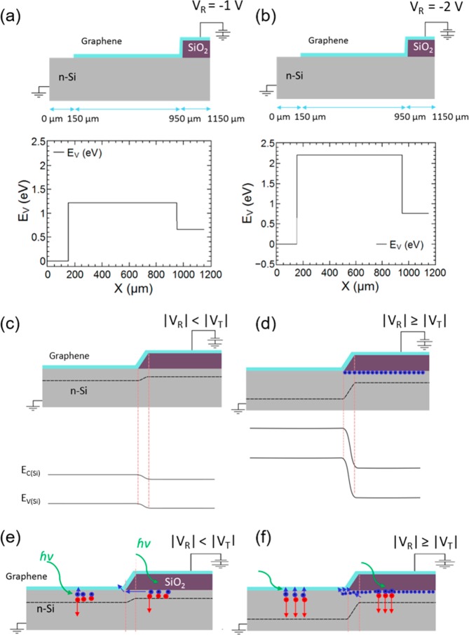
Figure 4.
Cross-section of the graphene–n-Si heterojunction diode with corresponding simulated plot of the valence band (EV) along the n-silicon, just at the top interface with graphene and SiO2 in reverse biased condition of (a) VR = −1 V (|VR| < |VT|) and (b) VR = −2 V (|VR| ≥ |VT|) in the dark. The conduction band (EC) will be parallel to the EV and shifted by the Si bandgap. Schematics, which show (c) formation of depletion layer in n-Si under graphene and G/SiO2 at |VR| < |VT| and (d) widening of depletion width in n-Si under graphene and formation of inversion layer in n-Si under SiO2 at |VR| ≥ |VT| in the dark and (e) and (f) under illumination. VR, VT, EC(Si), and EV(Si) indicate reverse voltage, threshold voltage, conduction band, and valence band of n-Si, respectively. Plotted dashed lines in n-Si region are representative of depletion layer. The formation of an inversion layer in Si, underneath G/SiO2 region, above a threshold reverse voltage results in a higher photocurrent in that region. The holes in the inversion layer may fill the trap states at the SiO2/Si interface, therefore, allowing more efficient collection of photogenerated holes. This results in a higher photocurrent with increasing reverse bias.

