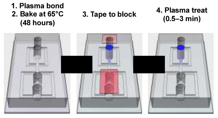
Fig. 1.

Fabrication steps for plasma wettability patterning. The device consists of a PDMS slab cast with microchannel structures bonded to a flat PDMS substrate. The chip is bonded by oxygen plasma treatment and baked for 48 hours to revert wettability back to hydrophobicity. Scotch-tape (red) is used to block plasma from entering certain inlet ports, while others are left open (blue). Oxygen species generated by the plasma diffuse into the open inlets, treating the channels near them to make them hydrophilic while leaving blocked channels hydrophobic. In this way, we are able to guide the plasma oxidation to achieve a desired wettability pattern.
