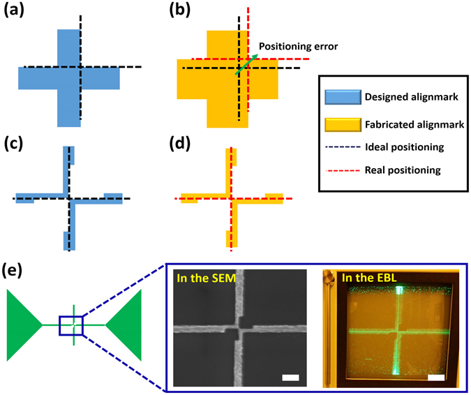
Figure 2.

Illustration of the idea on improving alignment and corresponding alignment marks. Since conventional alignment marks can be easily deformed by the proximity effect due to their geometry, complex 3D nanostructures could not be obtained easily. Therefore, new alignment marks are designed to achieve improved overlay accuracy. (a) Blue mark indicates designed marks and the black dashed line shows the ideal alignment position. (b) Yellow mark indicates fabricated marks and the red dashed line shows the actual alignment position. The errors come from the discrepancy between the designed mark and fabricated mark. The discrepancy results from a proximity effect of the electron beam. (c) Newly designed alignment mark. (d) Fabricated alignment mark. Because the alignment mark is composed of two bracket-shape structures and the structures meet at a point, the alignment mark is insensitive to the proximity effect. (e) Whole alignment mark design. Large triangle patterns are used to find the alignment mark easily and the center part is used for alignment. SEM image of the mark and a real picture of the screen during alignment steps in EBL mode. During scanning the alignment mark, we manually adjust the center point of the fabricated mark and virtual alignment mark shown as a solid green line. Scale bars represent 100 nm.
