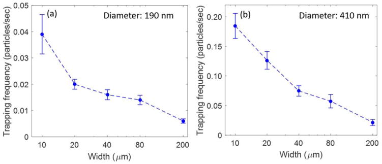
Figure 4.
Trapping frequency as a function of the width of the channel used for optical trapping of (a) 190-nm polystyrene particles, and (b) 410-nm polystyrene particles. The error bars represents the SEM with sample size of N=60 (W=10 μm), N=41 (W=20 μm), N=33 (W=40 μm), N=30 (W=80 μm), N=27 (W=200 μm) for 190 nm polystyrene nanoparticles and N=36 (W=10 μm), N=49 (W=20 μm), N=34 (W=40 μm), N=41 (W=80 μm), N=13 (W=200 μm) for 410 nm polystyrene nanoparticles

