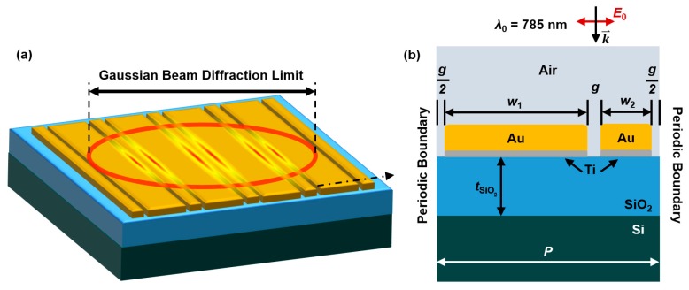
Figure 1.
Sketch of the dual-width plasmonic grating structure, on a Si substrate containing a layer of SiO2, with finite thickness: (a) shows a 3D representation of the structure and the generation of plasmonic hot spots within the area of a diffraction-limited Gaussian beam; (b) shows a 2D cross-section of the structure in (a) as designed in the computational models. The structure widths (w1 and w2), spacing width (g), period (P), and SiO2 thickness (tSiO2) are labeled, along with the incident wavelength (λ0), propagation direction (k), and electric field polarization (E0).

