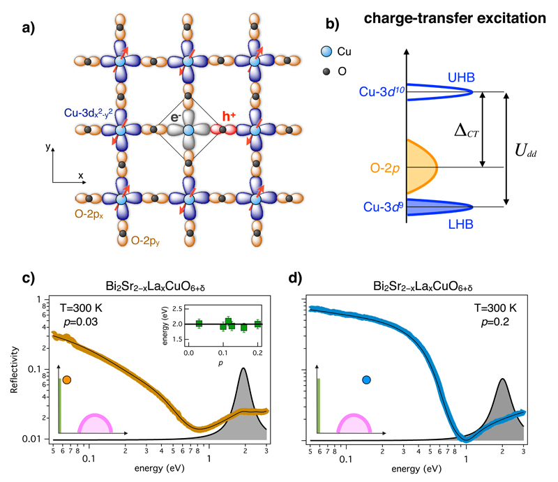
Figure 1. Charge-transfer excitation and optical properties of cuprates.
a,b) A sketch of the generic charge-transfer process in the Cu-O layer of copper oxides is shown. The upper (UHB) and lower (LHB) Hubbard bands, corresponding to the Cu-3d10 and Cu-3d9 configurations, are indicated c) The reflectivity curve, R(ω), of the underdoped sample is reported (yellow dots, taken from Refs. 29, 30). The black line is the fit to the data obtained from a model dielectric function which contains an extended-Drude term and three Lorentz oscillators that account for the high-energy transitions. The contribution of the first interband oscillator (ωCT), attributed to the charge-transfer process, to the total dielectric function is reported as a grey region. The inset displays ωCT as a function of the hole concentration. The left-bottom inset shows the position of the sample in the p-T phase diagram. The pink line represents the superconducting dome, while the green line indicates the CT insulating region. d) The panel displays the R(ω) of the overdoped sample (blue dots, taken from Refs. 29, 30). The black line is the fit of the model dielectric function to the data. The grey area represents the contribution of the CT oscillator to the dielectric function. The left-bottom inset shows the position of the sample in the p-T phase diagram.

