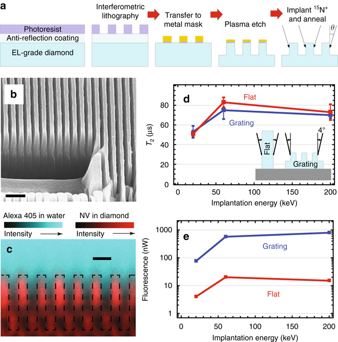
Fig. 2.

Diamond nanogratings. a Schematic of large-area nanofabrication process. b Scanning electron micrograph of 400 nm pitch diamond nanogratings. Focused ion beam etching prior to imaging enabled visualization of the nanogratings’ cross-section. Scale bar is 1 μm. c Confocal microscopy images reveal that fluorescence from dye-stained water originates from areas inside the nanograting grooves, confirming wetting. Dashed lines represent the estimated diamond–water boundary. Scale bar is 500 nm. d Comparison of T2, measured with the XY8-22 protocol, and e fluorescence intensity between flat and nanograting chips implanted at similar conditions. T2 can surpass ~100 μs with sufficient decoupling π-pulses (see Supplementary Note 2). Error bars in d represent standard error of the mean
