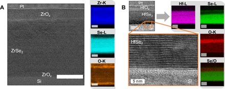
Fig. 2. Cross-sectional TEM and EDX mapping of native oxide formation.

(A) Cross-sectional TEM image of a smaller (<50 nm thick, <10 μm in lateral size) ZrSe2 flake following 3 days of ambient exposure, demonstrating both top-down and bottom-up oxidation into amorphous ZrOx, which partially consumes individual layers. Insets show that EDX elemental mapping demonstrates displacement of Se by O in oxidized regions. Scale bars, 20 nm. (B) Similar TEM images of a larger (>100 μm), thicker HfSe2 flake after 7 days of ambient exposure, with greater extent of top-down oxidation into HfOx, despite a pristine bottom interface with the Si substrate. Insets show EDX elemental mapping confirming complete chalcogen depletion, illustrated via overlay of O and Se signals. Scale bars, 50 nm.
