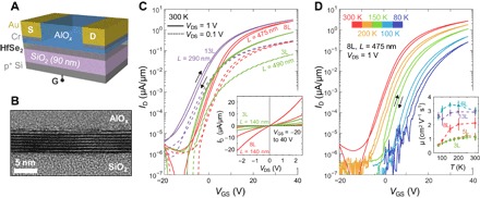
Fig. 3. HfSe2 transistors.

(A) Schematic of HfSe2 device, back-gated through 90-nm SiO2, and with ALD alumina used as both protective encapsulation and a ~25 Å interlayer in an MIS contact scheme (contact layers not to scale; capping alumina over contact metals not shown). (B) High-resolution TEM image of the channel of an 8L-thick HfSe2 device, with evidence of a partially oxidized top layer integrated into the capping oxide. (C) Room temperature transfer curves of HfSe2 transistors with varying channel thickness, demonstrating an on/off current ratio of ~106 at VDS = 1 V. Inset: Linear ID versus VDS plots for short-channel devices (L ≈ 140 nm) with 3L and 8L channels. All curves are dual sweeps from the origin, demonstrating low hysteresis (see arrows). (D) Temperature dependence of transfer curves for the 8L-thick HfSe2 device, from 80 to 300 K. The threshold voltage shifts higher as the sample is cooled. Inset: Field-effect mobilities of encapsulated 3L to 13L (~1.8 to 8.1 nm thick) HfSe2 devices.
