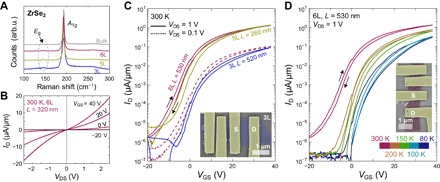
Fig. 4. ZrSe2 transistors.

(A) Low-power Raman spectra of ZrSe2 devices encapsulated by AlOx, from 3L to bulk, with minute shifts of A1g (~193 cm−1) and Eg (~145 cm−1) modes as the thickness is reduced (532 nm laser). arb.u., arbitrary units. (B) Hysteresis-free room temperature ID versus VDS forward and reverse sweeps for a 6L-thick ZrSe2 transistor (L = 320 nm) with a current density up to ~20 μA/μm. (C) Transfer curves of back-gated ZrSe2 transistors of varying channel thickness show lower current density in the thinnest (3L) devices. (D) Temperature-dependent transfer curves of the 6L device between 80 and 300 K show improved on/off current ratios with cooling (approaching 107) and forward shift in threshold voltage at lower temperatures. Insets are false-colored SEM micrographs of 3L and 6L devices, with source (S) and drain (D) contacts as labeled.
