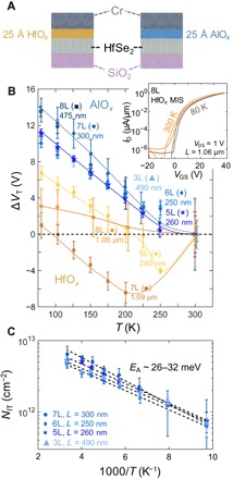
Fig. 5. Interfacial oxide engineering.

(A) Configuration of MIS contacts for HfSe2 transistors with 25 Å interlayers of either AlOx or HfOx ALD oxide (global 200 Å alumina capping is used for both). (B) Mean shift in threshold voltage ΔVT from the 300 K baseline for multiple HfSe2 devices cooled to ~80 K, contrasting the effects of AlOx (blue) and HfOx (orange) interlayers. VT was extracted from the linear intercept at the point of peak transconductance. Dashed lines are guides to the eye. Inset shows transfer characteristics of an 8L-thick HfSe2 device with HfOx interlayer at 80 and 300 K, demonstrating a minimal shift of VT and steeper turn-on behavior at lower temperatures. (C) Temperature evolution of estimated interfacial trap density NIT for multiple HfSe2 devices with AlOx interlayers, as calculated from ΔVT (see text). Dashed lines are fits to Arrhenius activation energies of 26 to 32 meV.
