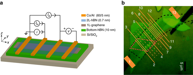
Fig. 1.

Device layout and measurement scheme. a A layer-by-layer schematic of the vdW heterostructure of the 2L-hBN/graphene/thick-hBN stack with FM cobalt electrodes. A measurement scheme is shown for the non-local spin transport measurements with a DC current bias I in and AC current i, applied across the injector contacts and a non-local differential (AC) spin signal v is measured using a lock-in detection technique. A DC current bias I d can also be applied in order to bias the detector contact. b An optical microscopic picture of the vdW heterostructure. Scale bar, 5 μm. The black-dashed line outlines the hBN tunnel barrier flake. The red-dashed line outlines the monolayer region of the hBN tunnel barrier flake (see Supplementary Note 1 for the optical microscopic picture of the tunnel barrier). A schematic of the deposited cobalt electrodes is shown as orange bars and the Co/hBN/graphene contacts are denoted by numbers 1, 2, .., and 13. The orange-dashed lines represent the unused contacts. Cobalt electrodes from 2 to 5 are either fully or partially deposited on top of the monolayer region of the tunnel-barrier flake, while the electrodes from 6 to 12 are exclusively deposited on the bilayer region. The width of the cobalt electrodes (2–12) is varied between 0.15 and 0.4 μm
