Fig. 4.

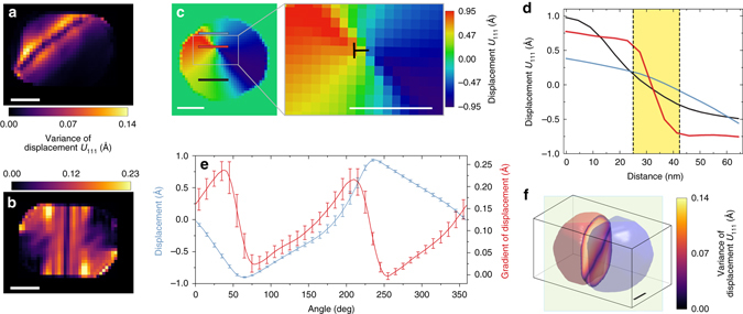
Identification of the domain wall and 3D rendering of nanorod as a defect within the nanoparticle. a Variance of displacement in the nanoparticle under the maximum electric field E 2 (223 kV cm−1), calculated in the vicinity of the domain wall. b Variance of displacement in the nanoparticle under the electric field E 3 (0 kV cm−1) calculated in the vicinity of the domain wall. c Map of displacement values and magnification of the boxed region for the nanoparticle at the slice shown as green plane in f for the state at field E 2 (223 kV cm−1). d Displacement values as a function of position of lineplots in c. e Angular dependence of the displacement field and of the gradient of the displacement measured along the defect line in f with error bars indicating standard deviation over the slices in the particle. f Rendering of the particle under field E 2 shows the 3D nanorod as a defect line whose 2D cross-section corresponds to the vortex core. Scale bars correspond to 60 nm
