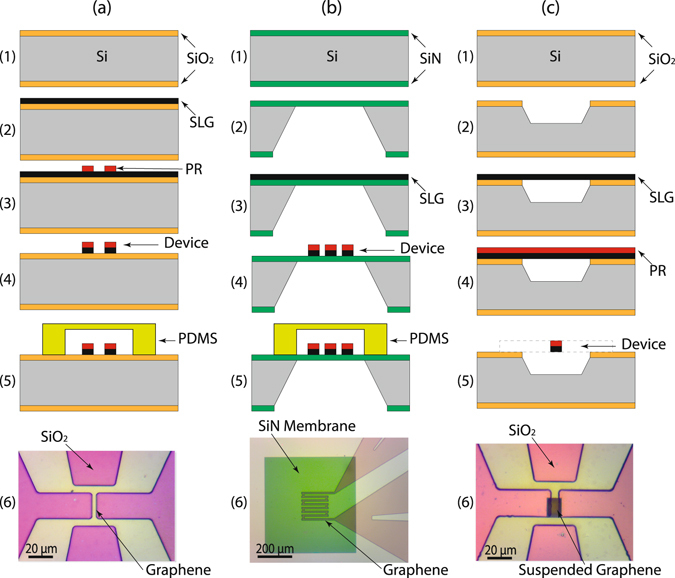
Figure 1.

Micro-fabricated SLG temperature sensor devices on three different substrates. (a) SiO2/Si substrate. Cross-sectional view of the fabrication process flow including: thermal growth of SiO2 (1), SLG transferring (2), device patterning (3), plasma etching of graphene (4), and (5) PDMS gasket protection of the sensor during PR removal at electrical contacts area. (6) Close-up picture of the completed device with 4-wire electrodes configuration. (b) SiN substrate. Cross-sectional view of the fabrication process including: (1) LPCVD SiN deposition, (2) defining membrane using the KOH etching from the backside, (3) SLG transferring, (4) device patterning using O2 plasma and (5) PDMS gasket protection of the sensor during PR removal at electrical contacts area. (6) Close-up picture of the completed device with the 4-wire electrodes configuration. (c) Suspended graphene. Cross-sectional view of the fabrication process flow including (1) thermal growth of the SiO2, (2) patterning the suspension pits using BOE etching of SiO2 followed by KOH etching of Silicon, (3) SLG transferring, (4) spin coating of PR and (5) device patterning using O2 plasma. (6) Close-up picture of the completed device with the 4-wire electrodes configuration.
