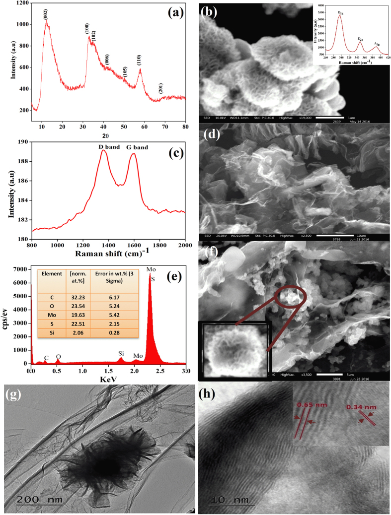
Figure 1.
(a) Diffraction pattern of as-prepared MoS2 nanoflowers with peaks at 13.55, 33.06, 35.22, 42.5, 49.82, 58.01, and 69.77. (b) SEM image of MoS2 nanoflowers (Inset Raman Spectrum of MoS2 nanomaterial with the band at 296.86, 346.87 and 390 cm−1). (c) Raman band at 1357 and 1596 cm−1 of 3D graphene. (d) SEM images of 3D graphene. (e) EDX spectrum of MoS2-3D graphene hybrid. The flower like MoS2@3D-graphene hybrid architecture has also been observed in SEM and high resolution TEM images shown in (f) and (g), respectively, which reveals the petals of MoS2 nano-flowers along with the 3D-graphene network effectively enhance the overall surface area that impacts on high storage capacity, (h) The hybrid interface is further confirmed by the HRTEM analysis where the lattice spacing are calculated to be 0.65 nm for MoS2 and 0.34 nm for graphene, respectively.

