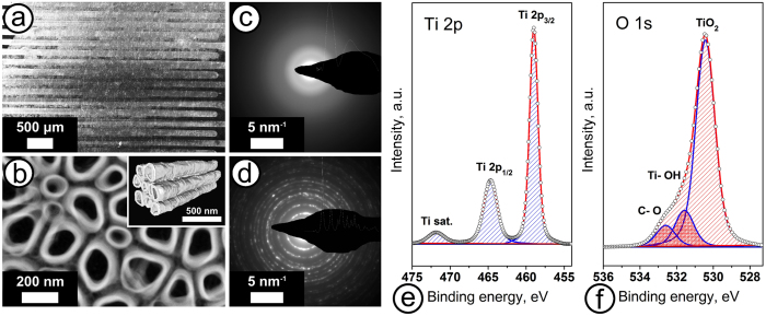
Figure 2.
Characterization of the TiOx NT arrays used in the multisensor chip: (a) SEM image taken of the chip surface covered with NT array; (b) HAADF-STEM image, the inset shows a surface rendering of the 3D STEM tomographic reconstruction viewed along the NT length; (c,d) SAED patterns of as-grown NTs and NTs annealed at 400 °C, respectively; (e,f) the XPS peaks related to Ti 2p (e) and O 1s (f) for the as-grown NTs, red lines show the envelope curves of all fitted peaks to compare with the experimental data (open circles).

