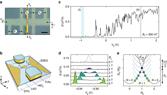
Fig. 1.

Device and zero-bias transport characteristics. a Optical microscope image of the split-gate device. The dark color shows the LSM hard mask and the STO is exposed to the LAO at the light colored regions forming a two-dimensional electron gas (2DEG). Scale bar is 5 μm. The 200 nm wide metal top gates are 1 μm apart. b Schematic of the device and formation of the QD close to pinch off with tunnel couplings ΓL,R to the 2DEG. c Conductance as a function of V g showing depletion for V g<−1 V. The two regions I and II, of weak and strong tunnel coupling, respectively, are investigated in detail. d Conductance G(V g) for V sd=0 in region I with varying magnetic field B y=0 to 6 T (solid lines). For clarity, traces are vertically offset by ~0.012 e 2/h. For B=0 a single peak is observed when increasing the bias to V sd=160 μeV (dashed). e Dependence of the ground-state energy on gate-induced charge N g=C g V g/2e for a single orbital with occupation N=0,1,2 and effective negative charging energy U. Solid lines represents B y=0 and dashed lines illustrate the Zeeman splitting of the odd-N state at B y=1–6 T. For E Z≥|U|, sequential single electron transport is allowed at the points marked with circles
