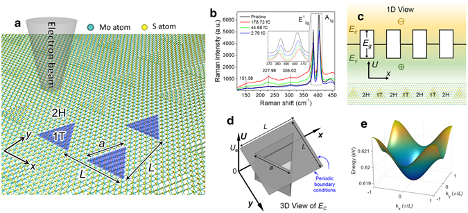
Figure 1.

1T phase quantum dot superlattice created on 2H phase monolayer MoS2 at room temperature. (a) Schematic of electron beam irradiation on 2H (semiconducting) phase MoS2 to trigger the transition of 1T (metallic) phase triangular MoS2 quantum dots, where is the lattice spacing (or pitch) and is the side length of the 1T phase triangle. (b) Raman spectra before and after electron beam irradiation. The inset shows the partially enlarged view of the E1 2g peaks and A1g peaks. As the electron beam irradiation dose increases, the intensities of E1 2g peak at 381.56 cm−1 and A1g peak at 404.82 cm−1 decrease, and E1 2g peak moves to lower wavenumbers and A1g peak moves to higher wavenumbers, which is different from the Raman peaks of MoS2′s defects24, 25. The intensities of the three peaks at 151.58 cm−1, 227.99 cm−1, and 305.02 cm−1 increase, which is the signature of the 1T phase MoS2 26–28. (c) Cross-sectional view of the periodic quantum well, where E C is the conduction band minima, E V is the valance band maxima, E g is the bandgap. (d) Two-dimensional periodic finite potential well model for calculating the emerging bandgap from quantum dot superlattice. The bottom of the triangular well is 1T phase MoS2. The top of the triangular potential barrier is the conduction band of 2H phase MoS2. is the height of the potential well. (e) Calculated band diagram of the first electron band for nm and nm.
