Fig. 1.
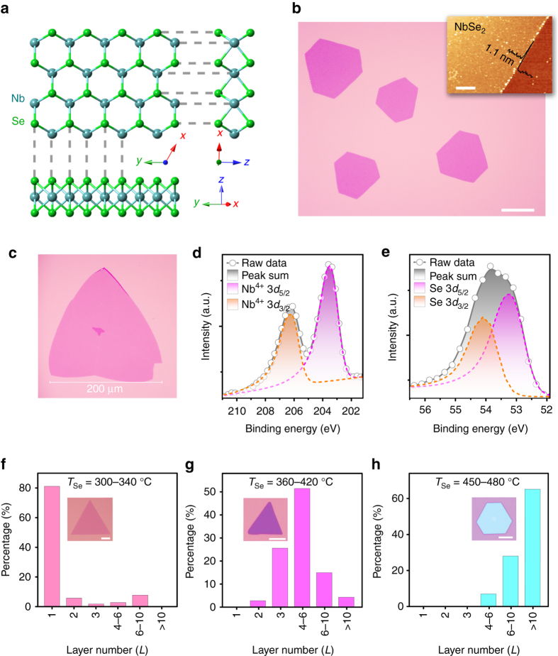
Atomic structure, morphologies, and characterizations of NbSe2 crystals. a Ball-and-stick model of monolayer 2H-NbSe2 viewed from three different directions. b Optical image of uniform NbSe2 crystals deposited on a SiO2/Si substrate. Scale bar, 40 µm. A representative AFM image (inset; scale bar, 1 µm) shows the typical thickness is 1.1 nm. c A monolayer NbSe2 crystal with edge length of 0.2 mm. d, e X-ray photoemission spectroscopy (XPS) spectra of the d Nb 3d and e Se 3d peaks from NbSe2 crystals deposited on SiO2/Si substrate. f–h Statistic thickness distributions and representative morphologies (inset) of NbSe2 crystals synthesized with T Se setting at f 300-340, g 360-420 and h 450-480 °C, respectively. Scale bars from inset of f–h are 20, 5 and 5 µm. Thickness of inset crystals of f–h are 1.1, 5.1 and 16.2 nm

