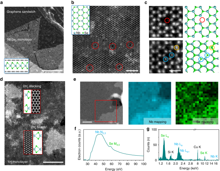
Fig. 2.
ADF-STEM images, EELS, and EDX characterizations of the as-synthesized NbSe2 atomic layers. a A low magnified annular dark-field scanning transmission electron microscope (ADF-STEM) image showing a large region of monolayer NbSe2 encapsulated by the graphene sandwich. The schematic is shown in the inset. b Atomic resolution ADF-STEM image of the hexagonal NbSe2 lattice. Diselenium vacancies are highlighted by red circles. The inset of panel b shows the structural model of 2H-NbSe2, with cyan and green color indicating Nb and Se atoms, respectively. c Different point defects in monolayer NbSe2 and their atomic models. Diselenium vacancy, monoselenium vacancy, and anti-site defect SeNb are highlighted by red, blue, and yellow circles, respectively. d Atomic resolution ADF-STEM image of two bilayer islands in NbSe2, showing the coexistence of 2H a and 2H c stacking sequence. The insets are corresponding atomic models and simulated STEM images. e STEM image of a large region of NbSe2 used for the collection of electron energy-loss spectroscopy (EELS) and energy-dispersive X-ray spectrometry (EDX) spectra. The collected region is highlighted in red square. Nb and Se EELS mapping are provided next to it. f Typical EELS and g EDX spectra of the region shown in e. The Cu signal in the EDX spectra comes from the Cu grid. Scale bars, 500 nm (a), 2 nm (b), 0.5 nm (c), 5 nm (d), 50 nm (e)

