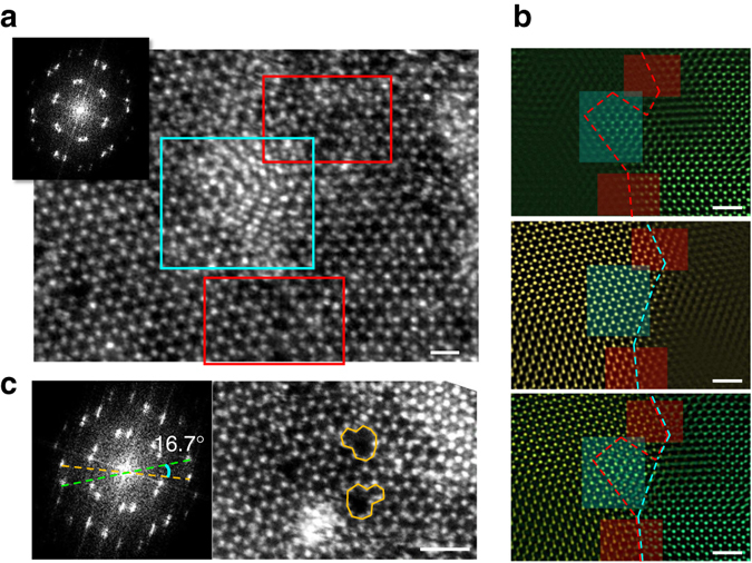
Fig. 3.

ADF-STEM images of the grain boundary in monolayer NbSe2. a A tilted grain boundary with misorientation angle of 11°. Both atomically sharp lateral interconnected (red rectangle) and vertically stacked (blue rectangle) boundary regions are found to coexist. The inset shows the fast Fourier transformation (FFT) of the image. The distorted polygons are also highlighted in the red rectangle. Scale bar, 0.5 nm. b Selected FFT-filtered image of the two domains and their overlap images. The overlapped image confirms the coexistence of the two types of grain boundaries. Scale bar, 1 nm. c Similar tilted grain boundary without an overlapping region nearby. The orange lines indicate the five-seven dislocation pairs, which is consistent with the theoretical predictions of the grain boundary structure. Scale bar, 1 nm
