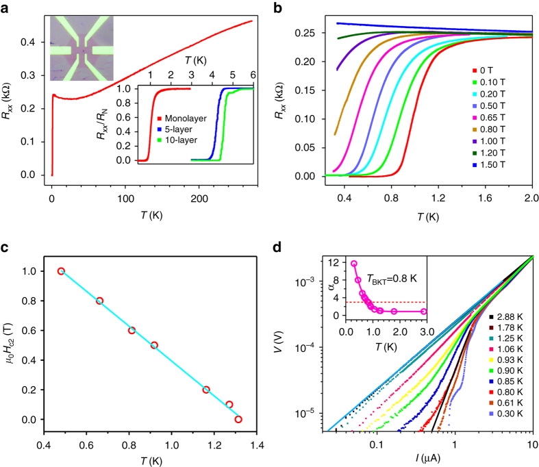
Fig. 4.
Superconductivity in monolayer NbSe2 devices. a Temperature dependence of the longitudinal resistance R xx for sample A—a monolayer NbSe2 device. Upper left inset: Optical image of a typical graphene protected monolayer NbSe2 device. Lower right inset: Superconductivity in monolayer, 5-layer and 10-layer NbSe2 devices. b Superconductivity of sample A in different magnetic fields. c Temperature dependence of the upper critical field H c2. The solid line is the linear fit to H c2. d Voltage–current (V-I) characteristic at different temperatures on a logarithmic scale. The solid blue line indicates the Ohmic behavior at high temperature. The solid black line represents the expected V∝I 3 behavior at the Berezinskii-Kosterlitz-Thouless (BKT) transition. The inset shows the temperature-dependent exponent deduced from the power-law behavior, V∝I α. As indicated by the red dashed line, α approaches 3 at T = 0.8 K

