
Figure 3.
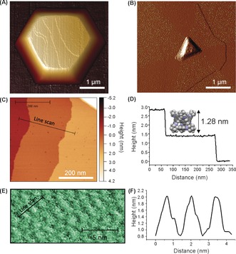
AFM analyses of surfaces of oriented cage crystals. A) AFM image of a defect‐free oriented cage crystal on silicon wafer. B) AFM PeakForce error image of a quickly‐grown oriented CC3 crystal showing the segments of the hexagonal crystal. C),D) Line scan of individual terrace steps from (B) on top of the crystals showing a step height of 1.41±0.18 nm, with a space‐filling model of CC3 shown to scale of the y axis. E) AFM topographic image of a well‐grown oriented cage CC3 crystal. F) Height profile along the pathway as shown in the image of (E).