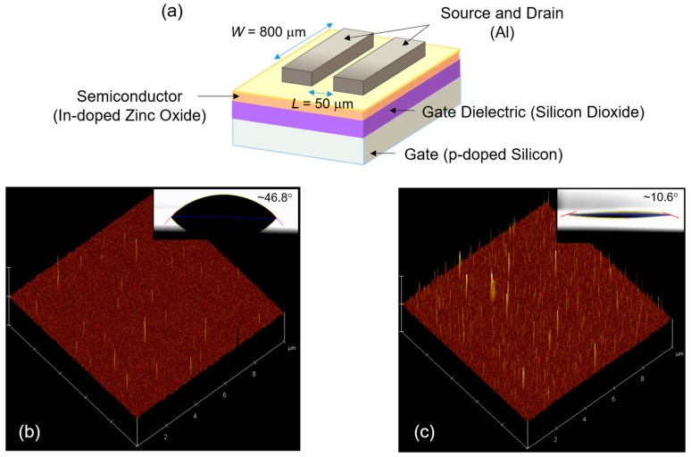
Figure 1.
(a) Schematic representation of the fabricated In-doped ZnO TFT having the channel length (L) and width (W) of 50 μm and 800 μm, respectively. Atomic force microscope images (10 × 10 μm) of the (b) pristine and (c) O2 plasma-treated SiO2 dielectric layers. The insets show the contact angles of both layers.

