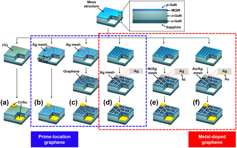
Figure 7.
Schematic illustration showing fabrication process of LED devices, using six types of TCLs: (a) 150-nm-thick ITO (“ITO”), (b) 150-nm-thick Ag mesh (“Mesh”), (c) a graphene layer on 150-nm-thick Ag mesh (“GR on Mesh”), (d) 150-nm-thick Ag mesh on a graphene layer (“Mesh on GR/Ag doping”), (e) 150-nm-thick Ag mesh and 5-nm-thick Ni mesh on a graphene layer (“Ni doping”), and (f) 150-nm-thick Ag mesh and 5 nm-thick Au mesh on a graphene layer (“Au doping”).

