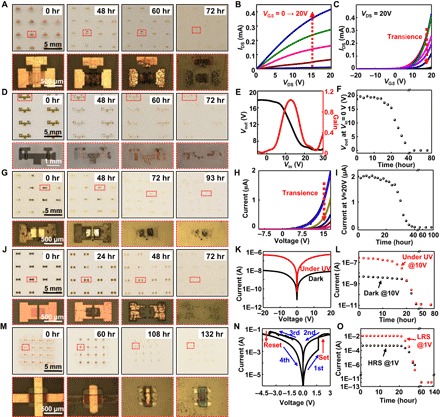
Fig. 6. Dissolution behaviors of the active devices of the moisture-triggered transient devices.

(A) Optical images showing the time-sequential dissolution of the TFTs. The bottom frames are the magnified images. (B) Measured current-voltage (I-V) characteristics of a TFT before transience starts. (C) Measured transience of the transfer curves of the TFT. (D) Optical images showing the time-sequential dissolution of the logic gates. The bottom frames are the magnified images. (E) Measured voltage transfer curve and gain of the inverter before transience starts. (F) Measured transience of the output voltage of the inverter at Vin = 0 V. (G) Optical images showing the time-sequential dissolution of the diodes. The bottom frames are the magnified images. (H) Measured I-V curves of a diode before and after transience starts. (I) Measured transience of the current of a diode at V = 20 V. (J) Optical images showing the time-sequential dissolution of the photodetectors. The bottom frames are the magnified images. (K) Measured I-V curve of photodetector under UV and in the dark before transience starts. (L) Measured transience of the current of the photodetector at V = 10 V under UV and in the dark. (M) Optical images showing the time-sequential dissolution of the resistive memories. The bottom frames are the magnified images. (N) I-V characteristics of a resistive memory before transience starts. (O) The measured transience of the current of the resistive memory at V = 1 V at low-resistance state (LRS) and high-resistance state (HRS).
