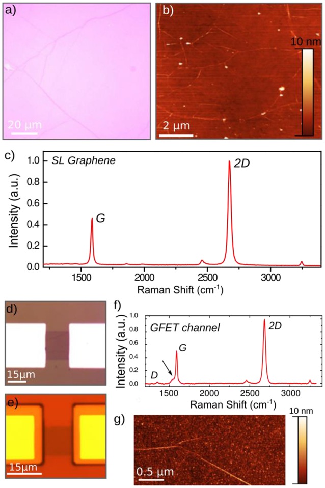
Figure 1.

Surface and structural characterizations of the CVD-grown graphene monolayers. (a) Optical micrograph of a typical graphene monolayer grown by pulsed CVD, after transfer on oxidized silicon (285 nm SiO2). (b) Atomic force micrograph of the graphene surface after transfer and annealing at 300°C for 3 h. (c) Raman spectroscopy underlying the characteristic Raman peaks of graphene monolayers (detailed in the text). Optical images of the graphene channel (20 × 15 μm2) before (d) and after (e) passivation. (f) Raman spectrum of the active graphene FET channel of the final device after contact passivation by photoresist. (g) Atomic force micrograph of the graphene FET channel after passivation.
