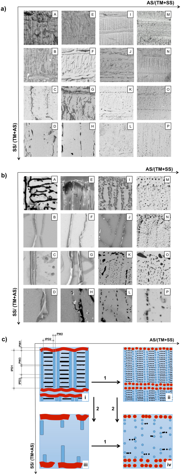
Figure 2.

(a) SEM images of PMMA patterns developed onto Si/SiOx substrates after the deposition of the 16 Ternary Solutions described in Table 1. Each photo is 91.8 × 91.8 μm, and is labelled according to the ID of the TS from which the pattern has been generated, as given in Table 1. (b) SEM images of the same PMMA patterns shown in Fig. 2a, accordingly labeled, with a higher magnification (each photo is in this case 10 × 10 μm). Only a few primary patterns have been imaged here (Panels E, I, M, N, K, O), as this would have implied a marked loss of information about the secondary and tertiary nanostructures (primary structures have sizes in the range of a few hundreds of nm-3 μm, while secondary-tertiary ones have sizes in the range on hundreds-tens of nm). Higher magnifications were not always possible to sudden damage experienced by the insulating PMMA under the electron beam at magnifications higher than 10.000x, hence for reasons of homogeneity all the images have been left to a relatively low magnification. (c) Cartoon illustration of the general trends in the topology development observed in Fig. 2a upon changing the TS composition. In panel (i) the labels have the following meaning: IPD stands for Inter-Pattern Distance, and the following number refers to primary (1), secondary (2) and tertiary (3) structures; PW stands for Pattern Width, with its numbering having the same meaning of the IPD notation. See text for more details.
