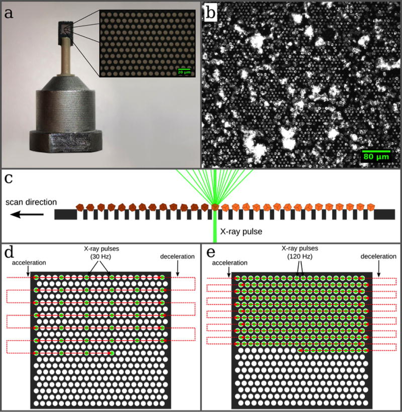
Figure 2. Design of the micro-patterned silicon chip and data collection strategy.

(a) The chip is attached to a plastic rod for the purpose of thermal isolation. The membrane part within the outer frame consists of micropores with diameters of typically 4 µm–8 µm, which are arranged in a triangular grid (a, inset). (b) The chip acts as a sample holder for more than 20,000 microcrystals, which largely organize themselves according to the pore pattern. (c) After loading, the microcrystals are scanned through the X-ray beam. By shooting through the micropores in the chips the interaction of the X-rays with any support material is further minimized. (d, e) Scanning strategies for measurements performed at room temperature and cryogenic temperatures, respectively (see text for details).
