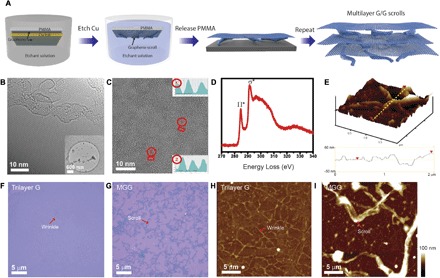
Fig. 1. Schematic illustrations and morphological characterizations of MGGs.

(A) Schematic illustration of the fabrication procedure for MGGs as a stretchable electrode. During the graphene transfer, backside graphene on Cu foil was broken at boundaries and defects, rolled up into arbitrary shapes, and tightly attached onto the upper films, forming nanoscrolls. The fourth cartoon depicts the stacked MGG structure. (B and C) High-resolution TEM characterizations of a monolayer MGG, focusing on the monolayer graphene (B) and the scroll (C) region, respectively. The inset of (B) is a low-magnification image showing the overall morphology of monolayer MGGs on the TEM grid. Insets of (C) are the intensity profiles taken along the rectangular boxes indicated in the image, where the distances between the atomic planes are 0.34 and 0.41 nm. (D) Carbon K-edge EEL spectrum with the characteristic graphitic π* and σ* peaks labeled. (E) Sectional AFM image of monolayer G/G scrolls with a height profile along the yellow dotted line. (F to I) Optical microscopy and AFM images of trilayer G without (F and H) and with scrolls (G and I) on 300-nm-thick SiO2/Si substrates, respectively. Representative scrolls and wrinkles were labeled to highlight their differences.
