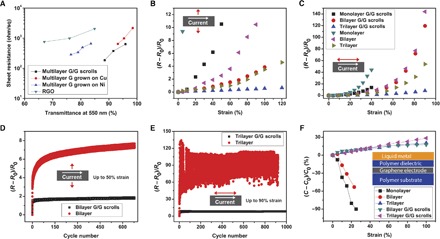
Fig. 2. Comparison of electrical and optical properties of MGGs and graphene.

(A) Four-probe sheet resistances versus transmittance at 550 nm for several types of graphene, where black squares denote mono-, bi-, and trilayer MGGs; red circles and blue triangles correspond with multilayer plain graphene grown on Cu and Ni from the studies of Li et al. (6) and Kim et al. (8), respectively, and subsequently transferred onto SiO2/Si or quartz; and green triangles are values for RGO at different reducing degrees from the study of Bonaccorso et al. (18). (B and C) Normalized resistance change of mono-, bi- and trilayer MGGs and G as a function of perpendicular (B) and parallel (C) strain to the direction of current flow. (D) Normalized resistance change of bilayer G (red) and MGG (black) under cyclic strain loading up to 50% perpendicular strain. (E) Normalized resistance change of trilayer G (red) and MGG (black) under cyclic strain loading up to 90% parallel strain. (F) Normalized capacitance change of mono-, bi- and trilayer G and bi- and trilayer MGGs as a function of strain. The inset is the capacitor structure, where the polymer substrate is SEBS and the polymer dielectric layer is the 2-μm-thick SEBS.
