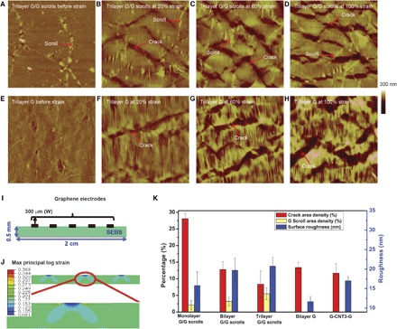
Fig. 4. Understanding the strain tolerance of conductivity of various graphene structures.

(A to H) In situ AFM images of trilayer G/G scrolls (A to D) and trilayer G structures (E to H) on a very thin SEBS (~0.1 mm thick) elastomer at 0, 20, 60, and 100% strain. Representative cracks and scrolls are pointed with arrows. All the AFM images are in an area of 15 μm × 15 μm, using the same color scale bar as labeled. (I) Simulation geometry of patterned monolayer graphene electrodes on the SEBS substrate. (J) Simulation contour map of the maximal principal logarithmic strain in the monolayer graphene and the SEBS substrate at 20% external strain. (K) Comparison of crack area density (red column), scroll area density (yellow column), and surface roughness (blue column) for different graphene structures.
