Fig. 3.
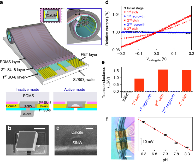
Calcite matrix as focal encapsulation for flexible Si FET. a Schematic representation of the tubular construct. Metal interconnects for FETs are passivated with two SU-8 layers, while SiNW can be encapsulated in calcite RE which is inserted in PDMS layer. FE of individual calcite heterostructure is exposed in the lumen for solution access. b SEM image of calcite RE-covered FET, recorded before PDMS deposition. Scale bar, 20 μm. c Cross-section SEM image showing the calcite/SiNW interface, scale bar is 100 nm. d, e Water-gate characteristics, showing relative drain-source current (normalized to the inactive state current at zero gate bias) vs. water-gate voltage (I − V wg) curves at a drain-source voltage of 0.1 V d and transconductances e during repeated etching-regrowth cycles. f Photograph of a microfluidic SiNW FET construct connected to polycarbonate tubings (left), allowing flow of mineralization precursors, etching buffer and solutions for pH sensing experiments. The calculated surface potential change of the Si FET sensor (right) vs. solution pH indicates that the response is linear and the slope of the fit (red dashed line) yields a response of 22.8 mV/pH. Scale bar, 5 mm. Error bar indicates standard deviation (n = 8)

