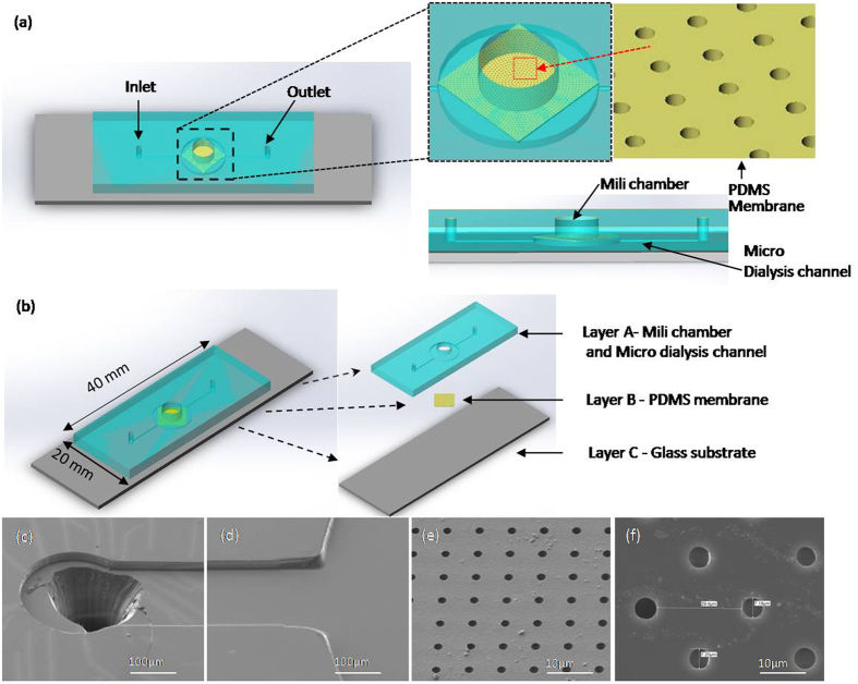
Figure 6.
(a) The 3D schematic of the 3D-µdialysis chip, including the enlarged image of the openmili chamber which is the staining region dwelling on the top of PDMS porous membrane with an array of holes, and the cross section view illustrating the micro dialysis channel beneath the porous membrane. (b) Assembly of a 3D µdialysis chip, including layer A: PDMS chip containing mili chamber and micro dialysis channel, layer B: PDMS porous membrane, and layer C: Glass substrate. (c) and (d) are the SEM images of the PBS solution inlet for micro dialysis channel and the entrance to the bottom of the mili chamber region (beneath the porous membrane). (e) and (f) are the SEM images of the PDMS porous membrane with an array of holes (7 μm holes with 20 μm space).

