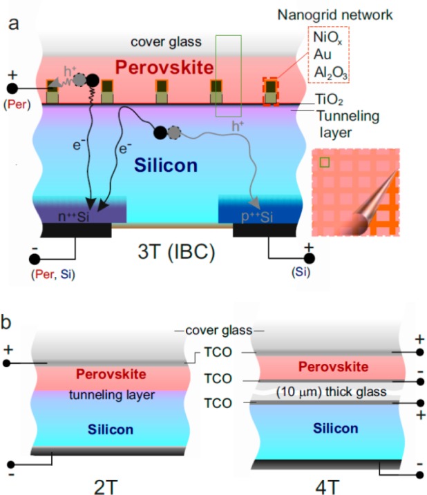
Figure 1.

Schematic designs of perovskite-silicon tandem solar cells. (a) Double back contact with three-terminal configuration (3-T (IBC)). The top open space (cover glass) is free providing opportunities for light trapping, antireflective coating, surface passivation, directional emission or enhanced photoluminescence outcoupling. The nanoscale embedded grid is composed of NiOx hole-transporting layer (orange), Au metal contact (dark-brown), and Al2O3 dielectric-insulating layer (light-brown). The negative polarity is shared between the perovskite (Per) and silicon (Si) cells in the n++Si (emitter) back contact silicon cell. Minority carriers from the silicon cell (e–) are collected then reinjected by the tunnel layer containing n++Si (front-floating emitter). The inset shows a schematic top view with 3D simulated unit cell indicated as a light-green box (half-pitch square size). (b) Traditional tandem configurations with two-terminal (2-T) and four-terminal (4-T) configurations; details in the Supporting Information. These cross-sectional views are not drawn to scale (perovskite thickness ranges between 0.05 to 1 μm, and the silicon is 180 μm).
