Figure 1.

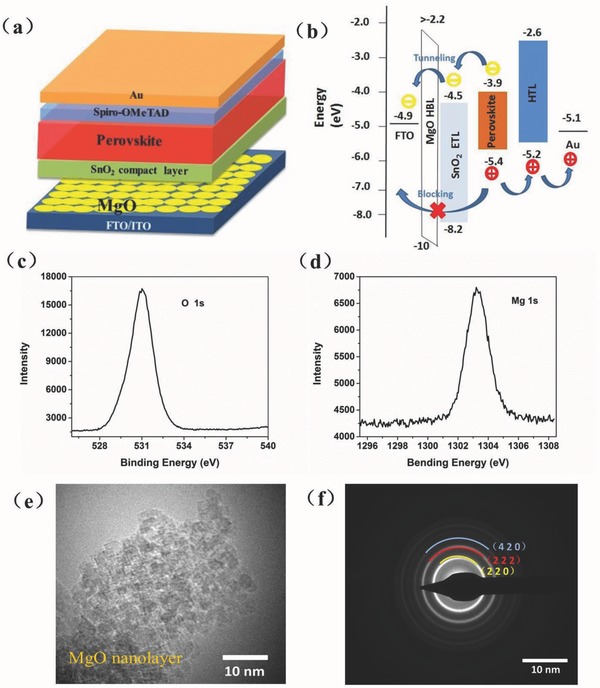
a) Schematic view of the device structure and b) energy band diagram of the device. XPS spectra of c) Mg 1s and d) O 1s peaks for an MgO film coated on a glass substrate. e) TEM and f) SAED images of an MgO nanocrystalline film.

a) Schematic view of the device structure and b) energy band diagram of the device. XPS spectra of c) Mg 1s and d) O 1s peaks for an MgO film coated on a glass substrate. e) TEM and f) SAED images of an MgO nanocrystalline film.