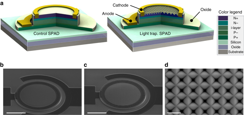
Fig. 1.
Structure of light-trapping SPAD. a Three-dimensional (3D) cross-sectional schematics of layer configurations of control (left) and light-trapping SPADs (right). The color legend shows the names of all the layers in both devices. The design thicknesses of layers from N+ to the bottom oxide layer of SOI substrate are sequentially listed 600, 300, 700, 200, 500, 220, and 400 nm for both devices. b, c Scanning electron microscope (SEM) images (45° view of top of structure) of control (b) and light-trapping SPADs (c) both with 50 μm diameter. Scale bar in both, 20 μm. d SEM image (top-down view) of inverse pyramid nano-structure on light-trapping SPAD. Scale bar, 1 μm

