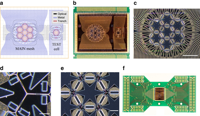
Fig. 2.

Fabricated hexagonal waveguide mesh chip. a Design layers (optical, electrical, and thermal) of the 7-cell hexagonal waveguide mesh and the auxiliary test cell. b Fabricated silicon on insulator (SOI) chip of footprint 15 × 20 mm. c Zoomed vision of the 7-cell hexagonal waveguide mesh. Scale bar of 2 mm. In the right bottom corner d zoomed image of an optical interconnection node of three tuneable basic units (TBUs). Scale bar of 100 µm. In the right bottom corner e zoomed image of a single hexagonal cell showing the Mach Zehnder Interferometer (MZI). Scale bar of 500 µm. In the right bottom corner, tuning heaters, and star-type thermal isolation trenches. f Printed circuit board with the waveguide mesh chip mounted and wired bonded
