Fig. 2.
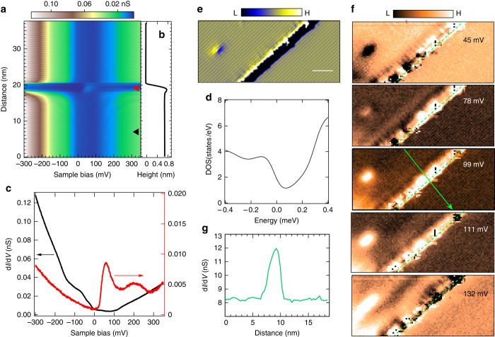
Spectroscopy of the edge states of WTe2. a Two-dimensional conductance plot of tunneling spectra measured along the black line in Fig. 1c, whose sectional line is shown in b, showing the emergence of edge states around the step edge. c Typical tunneling spectra measured at the step edge (red curve) and at a location at the inner terrace (black curve). The spectra were extracted from a at locations marked with red and black triangles, respectively. Measurement conditions of a: V s = 150 mV, I t = 200 pA and V mod = 3.5 mVrms. d Calculated density of states of bulk WTe2 with DFT. e Derivative STM image of a single layer high step edge along a-direction. The left terrace is the higher terrace. The scale bar corresponds to 5 nm. Measurement conditions: V s = 180 mV, I t = 200 pA. f Spectroscopic mapping of the imaged area in e at different voltages, showing the spatial distribution of the edge state with energy. Measurement conditions: V s = 180 mV, I t = 600 pA, V mod = 3.5 mVrms. g A sectional line profile extracted from f along the green line. The green-dashed lines in f mark the position of the step edge

