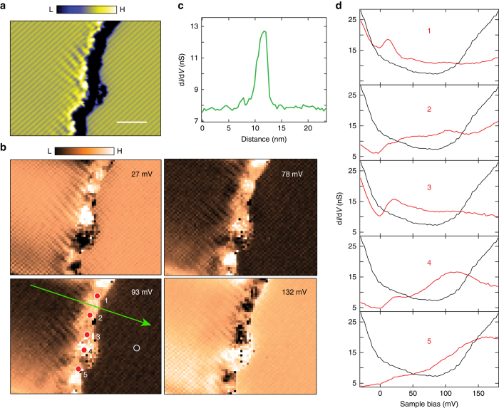
Fig. 3.
Edge states of WTe2 residing at an irregular shaped step edge. a Derivative STM image of a single layer high step edge with irregular shape. The scale bar is 5 nm. Measurement conditions: V s = 180 mV, I t = 200 pA. b Spectroscopic mapping of the imaged area in a at different voltages, showing the spatial distribution of the edge state with energy. c A sectional line profile extracted from b along the green line. d Tunneling spectra (red curves) at different locations of the step edge (red dots in b). The spectroscopy (black curve) of the inner terrace (black dot in b) is shown for comparison. Measurement conditions of b, d: V s = 180 mV, I t = 600 pA, V mod = 3.5 mVrms

