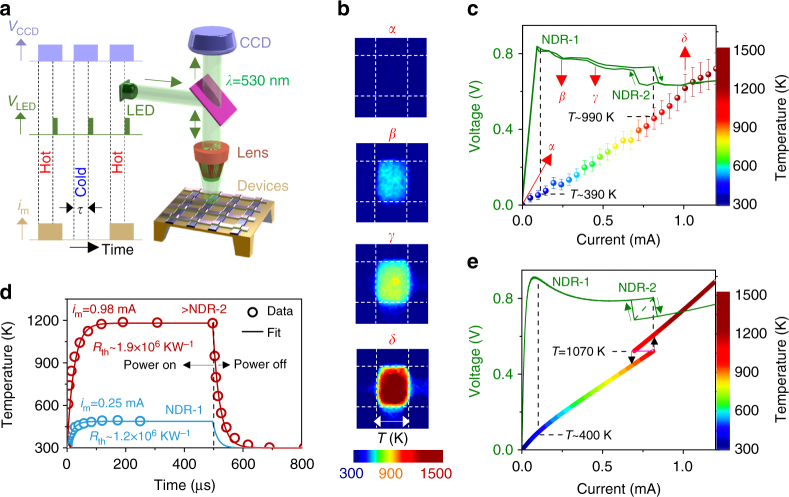
Fig. 2.
In operando thermoreflectance. a Schematic of the experimental setup. Synchronous operational pulse signals to the charge coupled device (CCD) full-field camera (V CCD), light-emitting diode (LED) (V LED), and the crosspoint devices (i m) are shown. “Hot” and “cold” refer to durations in which there is a current applied and not applied to the device, respectively. τ is the delay-time between the pump (application of i m) and probe (V LED). b Steady-state temperature maps of a single device at multiple constant current levels, with color-scale shown in c. Scale bar is 2 µm. c Experimental current–voltage curve of the device under measurement (using an increasing current sweep) and the corresponding average temperature within the crosspoint area at different current levels. Error bars represent the uncertainty in the measurement arising from calibration, noise, etc., (Supplementary Note 1). d Dynamic behavior of the average temperature within the crosspoint area of the same device upon application of a constant current (at time equal to 0) and upon withdrawal of the current (at time equal to 500 µs). e Simulated current–voltage curve and temperature of the device model (using increasing and decreasing current sweeps). Black arrows indicate hysteresis and temperature jumps predicted by the model. Pink solid line-segment indicates an abrupt jump in current that would occur upon a parametric temperature sweep. Green dashed-line segment is an abrupt jump in the current–voltage curve upon a parametric temperature sweep. Black dashed lines in c, e are used to indicate the temperature at the onset of the two regions of negative differential resistances (NDRs), namely, NDR-1 and NDR-2

