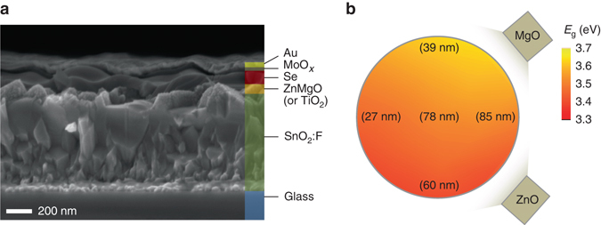
Fig. 1.

a Cross sectional scanning electron microscopy of the optimized device structure which consists of glass/SnO2:F/n-type buffer (ZnMgO or TiO2)/Se/MoOx/Au. Only 100-nm-thick Se absorber is used. b A schematic of combinatorial sputtering setup for accelerated studies on ZnMgO n-type buffer layers. A color map indicates the band gap (E g) of ZnMgO thin films measured by optical absorption spectra. The measured film thickness values in the map indicate a gradient of deposition rate
