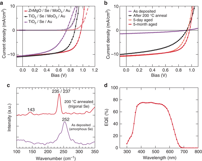
Fig. 2.

a As-measured current–voltage (J–V) characteristics of Se solar cell devices under dark (dashed lines) and illuminated (solid lines) condition, showing the effect of buffer and hole-transport layer. ZnMgO/Se/MoOx/Au, TiO2/Se/MoOx/Au, and TiO2/Se/Au devices are shown in red, black, and purple, respectively. b Illuminated J–V plots of ZnMgO/Se/MoOx/Au devices with as-deposited Se, annealed at 200 ˚C, 5-day aged after annealing, and 5-month aged after annealing Se are shown in purple, black, orange and red. c Raman spectra of as-deposited Se (purple) and annealed Se at 200 °C (red). The annealed Se shows convoluted peaks at 235 and 237 cm−1. d External quantum efficiency spectrum of a ZnMgO/Se/MoOx/Au device
