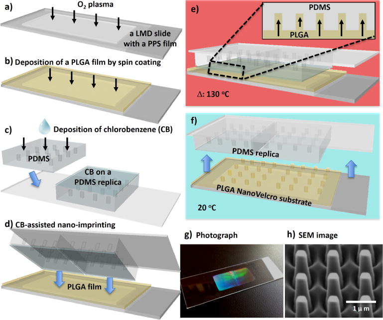
Figure 1.

Workflow developed for the fabrication of imprinted PLGA nanoVelcro substrate. (a) A laser microdissection (LMD) slide was first cleaned by O2 plasma; (b) a 1.0-μm-thick PLGA film was spin-coated onto the plasma-treated LMD slide; (c) chlorobenzene (CB) was sprayed onto PDMS replicates; (d) immediately after, the CB-coated replicates were pressed onto the spin-coated PLGA film; (e) the assembled layers were then heated to 130 °C. PLGA nanopillars were pulled into the nanofeatures on the bottom of the PDMS replicates, as a result of the absorbance of CB into PDMS matrix; (f) after the assembled layers were cooled to 20 °C, the PDMS replicates were peeled off from the substrate to give (g) an imprinted PLGA nanoVelcro substrate on an LMD slide; (h) SEM image shows the topography of the imprinted PLGA-nanopillar features.
