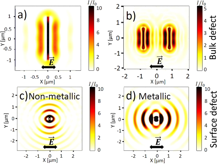
Figure 2.
Bulk defect: (a) Intensity distribution integrated over the period around a single void nanoplane nm, μm, nm. (b) Intensity distribution integrated over the period as a result of the coherent superposition of the scattered waves from two void nanoplanes nm, μm, nm, separated by 2 μm in x-direction. Surface defect: Intensity pattern integrated over the period from a single inhomogeneity (hemisphere with nm) (c) on the non-excited fused silica surface (), (d) on the excited metallic fused silica surface (). Laser wavelength is fixed to be nm.

