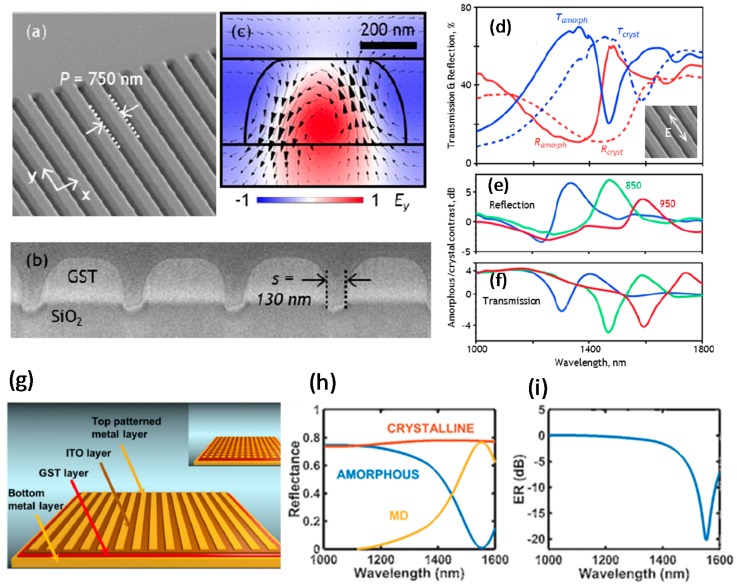
Figure 3.
GST-based metasurface with a grating nanostructure. (a) Tilted incidence and (b) cross-sectional SEM image of the nanograting in a GST225 film on an SiO2 layer; (c) Simulated spreading of y-component of the electric field in the xz surface for a nanograting unit cell at resonance; (d) Reflection and transmission spectra of the nanograting based on GST225 at both amorphous and crystalline phases. Calculated switching contrast of (e) reflection and (f) transmission dispersion of the TE mode at both of the GST225 phases; (g) Schematic illustration of the GST-based absorber-modulator using gratings for near infrared spectra; (h) The simulated reflectance curve with strips of Au top electrode and GST225 thin film in both recognized phases; (i) The optimized extinction ratio (ER) for the maximum modulation depth (MD = 77%) at 1550 nm. (a–f) are adapted from [1], with permission from © 2016 AIP Publishing LLC; and (g–i) are adapted from [38], with permission from © 2016 OSA. ER is described by the logarithm of the reflected power ratio, while MD represents the difference between the maximum and minimum reflected power.

